
EBSD Explained
Techniques
Applications
Hints and Tips
Technology
OXFORD INSTRUMENTS EBSD PRODUCTS
CMOS Detector RangeAZtecHKL Acquisition SoftwareAZtecCrystal Processing Software
There is a growing interest in the use of direct electron detection (DeD) for electron backscatter diffraction (EBSD), where the diffraction pattern is acquired directly via a pixelated semiconductor image sensor. This contrasts with the conventional approach of indirect electron detection (IeD), where incident electrons strike a scintillator (e.g. a phosphor screen), generating photons that are subsequently imaged using an optical camera system. Given that, in IeDs, both the conversion of electrons to photons and the detection of the photons using an optical camera can be relatively inefficient processes, and that some electron-counting DeD systems offer “single electron sensitivity” (i.e. detecting individual electrons as discrete particles so that the signal is completely free of any system noise), it would seem intuitive that DeD systems must offer the ultimate sensitivity for EBSD. However, reported results to date, using sensors such as Timepix and Timepix3, have not demonstrated any quantified improvement to sensitivity compared to the most sensitive IeD EBSD cameras such as the Symmetry S3 detector.
Having examined the topic of sensitivity already (see “fibre optics and sensitivity”), here we take a brief look at the physics of electron detection to understand better the sensitivities of an optimised IeD, such as the Symmetry S3 detector, and an electron-counting (EC) DeD. The results indicate that, contrary to popular belief, the indiscriminate detection of backscattered electrons of all energies using an EC-DeD actually results in a lower sensitivity than is possible with the Symmetry S3 IeD. This surprising result explains the lack of any sensitivity benefit from the use of DeD technology in EBSD applications to date.
Any EBSD analysis depends on detecting faint, low-contrast Kikuchi bands against a noisy background in the EBSP. Increasing the electron dose used to acquire the EBSP results in an increased signal to noise ratio (SNR), making the Kikuchi band signal more discernible from the background noise. Once above a certain dose (the detection limit), a threshold SNR is reached and the EBSP may be successfully analysed. The detection limit can also be influenced by the analysis strategy, with offline image enhancement or pattern correlation approaches resulting in lower detection limits than is usually achieved using real-time, Hough-transform based indexing.
The signal of interest in EBSD experiments, contributing to the formation of the Kikuchi bands in the EBSPs, is just a small fraction of all the backscattered electrons (BSEs) that impinge on the EBSD detector. It is well known that these diffracted electrons typically have energies within just ~ 1-2 keV of the primary beam energy, E0 [see reference 1]. The remaining fraction of BSEs (the majority) have a lower mean energy and do not contribute to the Kikuchi bands, forming only a diffuse background. If they are detected, then they only contribute to the noise in the diffraction pattern and thus reduce the overall SNR. For this reason, there has been significant interest in the use of some form of energy discrimination within EBSD detectors as a method to improve SNR [2 - 4]. Here we model the energy distribution of the BSEs in an EBSP and look at the energy response function of the detector itself, enabling a quantification of the relative sensitivities of IeD and DeD designs.
The energy distribution of BSEs in an EBSP, P(E), has been modelled using a Monte Carlo simulation [5], and the results are shown in the figure. P(E) describes the probability of a primary beam electron being scattered by the sample such that it impinges on the detector with an energy E. Although the exact position of the electron on the detector will affect the energy distribution, this effect is not significant for this analysis and hence an average is used for the whole diffraction pattern.
In addition, it is possible to estimate the fraction of BSEs with an energy E that has been diffracted and contribute to the Kikuchi band formation [6], and this is referred to as D(E). There is some debate about the exact energy distribution of diffracted electrons but, for the purposes of comparison between detector types, it is possible to use an estimate of D(E) that will be applicable for both strongly and weakly diffracting samples. It is clear from the graph (red curve) that the diffracted electrons predominantly have an energy that is close to the primary beam energy (in this case 20 keV), in contrast to the energy distribution of all BSEs (black curve).
It is possible to determine the number of electrons that contribute to the diffraction contrast as (sample dose) * P(E) * D(E), and from that the signal of interest can be calculated as the area under the red curve in the figure.

Backscattered electron energy distributions P(E), and P(E).D(E) used for SNR calculations in this work. (Monte Carlo simulations for Si sample; 70° tilt; SEM primary beam energy, E0 = 20 keV.)
In addition, since the shot noise inherent to the total flux of BSEs can be determined from Poisson statistics [7], the SNR at the input to the detector is simply the ratio between the input signal and the shot noise. However, more critically, the SNR within the diffraction pattern itself will depend on the response of the detector to electron energy: the detector energy response function.
[1] A. Winkelmann, T. Ben Britton, and G. Nolze (2019), “Constraints on the effective electron energy spectrum in backscatter Kikuchi diffraction.” Phys. Rev. B, vol. 99, no. 6, p. 064115.
[2] Abhishek Bhattacharyya, John A. Eades (2009), “Use of an Energy Filter to Improve Spatial Resolution of Electron Backscatter Diffraction.” Scanning, vol. 31, 114-121.
[3] US Patent US8890065B2: Apparatus and method for performing microdiffraction analysis
[4] Vespucci, S., Winkelmann, A., Naresh-Kumar, G., Mingard, K., Maneuski, D., Edwards, P., Day, A., O’Shea, V., Trager-Cowan, C. (2015). “Digital direct electron imaging of energy-filtered electron backscatter diffraction patterns.” Physical Review B 92, 205301
[5] X. Llovet and F. Salvat-Pujol (2016), “PENEPMA: a Monte Carlo programme for the simulation of X-ray emission in EPMA.” IOP Conf. Ser. Mater. Sci. Eng., vol. 109, p. 012009.
[6] F. Ram and M. De Graef (2018), “Energy dependence of the spatial distribution of inelastically scattered electrons in backscatter electron diffraction” Phys. Rev. B, vol. 97, no. 13, pp. 1–5.
[7] L. Reimer (1998), Scanning Electron Microscopy, vol. 45. Berlin, Heidelberg: Springer Berlin Heidelberg.
Electron-counting detectors are systems with very high electron gain so that the signal generated by a single electron is much greater than the system noise. In addition, fast, on-pixel electronics discriminate the signal from the noise (using an appropriately set, low-energy threshold) to produce a digital count of each single electron event before the next electron arrives. Although this eliminates system noise, the low-energy threshold means that there is no discrimination between high-energy electrons (such as those that contain diffraction information) and low-energy electrons (contributing to the noise). Each detected electron is given equal weight, so the effective contribution of electrons to the EBSP will be very similar to the energy distribution of all BSEs (as shown in the graph in the “EBSD Energy Distribution” tab) – this is shown by the black curve in the figure:
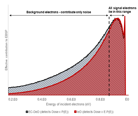
Effective BSE energy spectra as detected using optimised IeD and EC-DeD cameras, as a function of the energy of incident electrons (the plots have been scaled to the same peak value)
Indirect electron detectors are typically not suitable for electron counting; rather than producing a noise-free, digital count of incident electrons, their output is formed from an analogue integration of the total charge induced by the incident electrons, and they are referred to as Charge-Integrating (CI) detectors. CI-DeD cameras are also available and are commonly used in transmission electron microscopy, with limited investigation into their potential for EBSD applications [See reference 1]. CI detectors are not free from system noise, but for optimised high-gain systems (as exemplified by the Symmetry S3 detector) the system noise is insignificant except at very low electron doses. This is detailed in a separate technical note “High Sensitivity EBSD Detectors” available here.
Importantly, in CI detectors, the output is proportional to the energy of the incident electrons (with the constant of proportionality being the electron gain, G). This linear relationship means that the higher-energy part of the measured spectrum is preferentially weighted compared to the lower-energy electrons, as shown by the red curve in the figure above. Given that most diffracted electrons have an energy close to the incident energy, this means that a high-gain charge-integrating IeD will have a superior SNR for diffracted electrons compared to a simple, low-threshold electron-counting DeD.
It is possible to compare quantitatively electron-counting DeD and charge-integrating IeD EBSD cameras by calculating the ratio between their respective sensitivities, as determined using the modelling approach outlined above. The sensitivities for the detectors (SEC-DeD and SIeD) are invariant for a fixed sample and experimental condition, and have the following ratio:
SIeD / SEC-DeD = 1.4
This means that an optimised, high-gain IeD such as the Symmetry S3 EBSD detector will be approximately 1.4 times more sensitive than a simple, low-threshold EC-DeD.
It is expected that at very low doses (when the system noise becomes more influential) and at very low primary beam energies (when the phosphor screen has a lower efficiency of photon generation) the sensitivity advantages of an optimised IeD will be reduced.
[1] A. J. Wilkinson, G. Moldovan, T. B. Britton, A. Bewick, R. Clough, and A. I. Kirkland (2013), “Direct detection of electron backscatter diffraction patterns,” Phys. Rev. Lett., vol. 111, no. 6, pp. 1–5.
There are many different terms that are used when discussing detector technologies and, in particular, the different types of direct electron detectors. This table will help you to differentiate between a hybrid pixel detector and monolithic active pixel sensor!
CMOS – Complementary Metal Oxide Semiconductor – the most widely used sensor technology.
Monolithic Active Pixel Sensor (MAPS) – a CMOS-based technology in which each active pixel has one or more amplifiers. Such sensors are entirely within a single layer of Si and can have relatively small pixel sizes, resulting in higher pixel numbers but lower dynamic range.
Hybrid Pixel Detector – a detector that includes a semiconductor sensor layer bump-bonded to a processing CMOS electronics layer. Pixel sizes are usually larger, limiting overall pixel numbers, but enabling higher dynamic range.
Pixel Array Detector (PAD) – another term for a Hybrid Pixel Detector.
Electron-Counting Direct Electron Detector (EC-DeD) – a type of DeD that enables the counting of individual electrons, with an elimination of system noise when imaging at very low doses.
Charge-Integrating (CI) Detectors – a detector type that continuously integrates the charge on the sensor caused by incident electrons. Most common for high-dose applications, both using direct and indirect electron detector technologies.
SNR – Signal to Noise Ratio – the ratio between the output signal and the noise present in the output signal. This shows the performance of a sensor in response to a particular exposure.
Dynamic Range (DNR) – the ratio between the maximum output signal level and the noise floor at minimum amplification. The DNR determines the number of signal levels that a sensor can resolve.
Shot Noise – also referred to as “Poisson Noise”, this is caused by the discrete nature of the individual electrons, resulting in signal fluctuations. It will influence the signal to noise ratio at higher signal levels.
Read Noise – the noise caused by the electronics of the sensor; this will determine the lowest number of electrons that the sensor will be able to detect. Sometimes referred to as “System Noise”.
Dark Current (Noise) – this is a current generated within the sensor, independent of the detection of any electrons. The dark current is highly dependent on the operating temperature, but is usually negligible over the short exposure times typical for EBSD.
© Oxford Instruments 2026