EBSD Explained
Techniques
Applications
Hints and Tips
Technology
OXFORD INSTRUMENTS EBSD PRODUCTS
CMOS Detector RangeAZtecHKL Acquisition SoftwareAZtecCrystal Processing Software
The beam-sample-detector geometry is an important consideration when setting up an Electron Backscatter Diffraction (EBSD) analysis. Optimising the geometry will ensure the best results for a wide range of applications, although it may be necessary to compromise on some aspect of the set-up to accommodate unusual samples or special applications.
The parameters to consider when setting up the EBSD experiment are as follows:
These parameters can be adjusted either on the SEM (e.g. by adjusting the stage position) or by moving the EBSD detector (insertion/retraction or, on detectors such as the Symmetry S3, by adjusting the elevation to move the phosphor screen up or down). The image to the right summarises these variables for a typical EBSD set up.
In the tabs below you can read more about how best to adjust these parameters, plus some more details on the special case of EBSD in transmission: transmission Kikuchi diffraction (TKD).

Schematic illustration showing the main variables associated with the geometry set-up for EBSD experiments
Historically, a tilt of approximately 70.5° was used in early EBSD experiments because at that tilt angle, the <114> direction for a silicon (100) crystal would be positioned at the pattern centre, making system calibration much easier.
Modern EBSD systems perform the geometry calibration automatically, but we still use a tilt angle of ~70° from horizontal for 2 reasons:
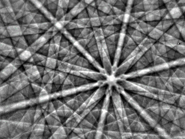
The series of images below show the effect of tilting the sample to lower tilt values. Note the progressive loss of signal to noise, plus the inversion of Kikuchi band contrast in the lower parts of the EBSP.


EBSD patterns collected from Si at different sample tilt angles. Left – 70°, Centre – 60°, Right – 50°.
The tilt angle can be set by tilting the SEM stage to the desired value, or by using a pre-tilted holder. The choice will depend very much on the SEM in question and the set-up of the EBSD detector relative to the stage tilt axis. The advantage of tilting the stage is that, for most SEMs, the sample can then be moved in the plane of the sample surface (i.e. the tilted X-Y plane) and the WD and beam-sample-EBSD detector geometry will remain constant.
There has been some recent exploration of the potential of performing EBSD at very low sample tilt angles or in a horizontal geometry. Early studies showed significant problems with contrast reversal, but the use of direct electron detection technology, coupled with electron energy thresholding, can circumvent this problem. However, the signal to noise ratio is significantly reduced and hence extremely high electron doses are required for successful analyses using this low-tilt geometry.
The working distance is an important consideration when setting up an EBSD experiment, primarily because it will affect the position of the pattern centre on the EBSD detector’s phosphor screen (and thus the strength of the signal).
For most standard experiments, the optimum position of the pattern centre is about ¾ up the phosphor screen, but this will be affected by the beam energy and the atomic number of the material to be analysed.
When selecting the optimum WD, consideration needs to be made about the following factors:
The series of images below show the changes in EBSP quality when moving from a 14.9 mm WD to a 22.5 mm WD. At the shorter WD, the EBSP is relatively noisy at the bottom of the pattern, whereas at the longer WD it is the upper part of the pattern that is noisy. EBSD indexing would still be possible for all of these geometries, but the loss of signal would become more significant the further the WD is extended beyond the optimum position.


EBSD patterns from ferrite collected at different working distances. Left – 14.9 mm, Centre – 18.9 mm, Right – 22.5 mm. The position of the pattern centre is marked by the green cross.
When an EBSD detector is installed, typically the engineer will set a physical safe limit for the detector insertion that is recommended for that particular SEM chamber. This fully inserted position will normally have the detector’s phosphor screen close enough to the sample to subtend a large solid angle (>90°). Depending on the size of the phosphor screen, this will usually equate to a detector distance in the range of 15 – 30 mm.
However, it is not always beneficial to insert the detector to its fully inserted position and to work with the shortest possible detector distance. The following factors should influence the decision on what detector distance is best for a particular application:


Channelling contrast images of a duplex stainless steel collected using forescatter detectors below the EBSD detector phosphor screen. Left- full insertion, with the signal dominated by topography from the sample preparation. Right – detector retracted 10 mm, providing much greater crystallographic contrast.
To perform successful TKD analyses using a standard off-axis geometry, setting up in an optimised beam-sample-detector geometry is necessary. Unlike conventional EBSD, for TKD analyses the sample should be positioned in a horizontal geometry, or slightly tilted away from the EBSD detector.
The ideal geometry is shown in the annotated chamberscope image on the right.

Chamberscope image showing the ideal geometry for off-axis TKD analyses
© Oxford Instruments 2025