In-Situ Electron Backscatter Diffraction (EBSD)
For most microstructural analyses, we characterise the microstructure after any thermal or mechanical processing has been completed. Then, in order to understand the development of the microstructure, theoretical approaches are required which combine knowledge about slip systems, deformation mechanisms and phase diagrams. However, if it is possible to observe microstructural changes as they happen, then we will gain a far greater understanding of the key processes that define the physical properties of the material.
For this we need to perform in-situ Electron Backscatter Diffraction (EBSD) inside the scanning electron microscope (SEM), and observe the evolution of the microstructure in response to changes in strain or temperature. In-situ EBSD is not always simple: there are likely space limitations in the SEM chamber, restrictions on the sample size and shape and numerous other experimental challenges. Dedicated heating, cooling and testing stages are now widely available for performing in-situ experiments in the SEM, and many of these are specially modified to function at the high sample tilts required for EBSD. The latest high sensitivity, high speed CMOS-based EBSD detectors are ideal for in-situ experiments, capturing rapid maps of the microstructure in a matter of seconds, so that researchers can accurately track the microstructural changes as they occur.
There are specific challenges associated with in-situ EBSD, as follows:
Infrared (IR) radiation from samples and heating elements - Although dependent on the sample and the heating stage design, IR becomes a significant problem typically at temperatures exceeding 500-600 °C. These problems can be eliminated by the use of high temperature phosphor screens (see the next section)
Shadowing of the EBSD detector - This can be because of components of the in-situ stage, such as heat shields or parts of the loading/heating mechanisms. Having a detector that can rapidly adjust its elevation is a major advantage in such cases, as the geometry can be adjusted to eliminate any shadows. Alternatively dynamic shadow-masking tools are available in some commercial systems.
Surface topography - This is typically a problem during high strain experiments: intracrystalline deformation will cause grain-by-grain variations in the surface height, resulting in imaging and shadowing problems during analyses
Lattice distortion - During straining experiments, the build up of dislocations and associated localised distortion of the crystal lattice can make any EBSD analysis particularly challenging (the EBSD patterns will become increasingly blurred and distorted, becoming difficult to index using standard Hough-based techniques)
Frost build up - For cooling experiments (e.g. for EBSD on ice samples), particular care must be taken during the sample transfer into the SEM chamber, otherwise the surface may suffer from significant build up of frost which will prevent effective EBSD measurements
Sample drift - During experiments, when the sample may be under load or at an elevated temperature, sample drift can be a significant issue. This will make it more challenging to correlate data during post-experiment analyses, but can be minimised by the use of the latest high-speed detectors or drift-correction tools
Despite these changes, in-situ EBSD can give exceptional results on a wide range of materials. The example to the right shows in-situ annealing of a deformed Al sheet: the series of EBSD datasets were collected over a period of 15 hours at a temperature of 295°C and show the progressive recrystallisation of grains from the sample edges towards the centre.
High Temperature Phosphor Screens
High temperature EBSD experiments are particularly challenging due to the excess IR radiation that can be emitted from the sample and the heating elements. The IR signal floods electron detectors (e.g. solid state backscattered and forescattered electron detectors) and, for a regular EBSD phosphor screen, will create many artefacts in the pattern that make routine background processing and subsequent indexing very challenging.
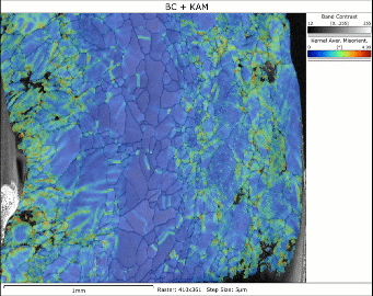
Animation showing a series of kernel average misorientation (KAM) maps of a bent Al sample, held at a constant 295°C. The darker blue colours indicate lower levels of plastic strain (i.e. recrystallised grains).
The image below shows the extent of IR radiation during a high T EBSD experiment, as imaged using an (IR sensitive) chamberscope. The EBSD pattern shows bright regions caused by imperfections in the phosphor coating: these will be dynamic during an experiment and are thus impossible to eliminate using correction with a single, stored static background.
Problems caused by IR radiation during in-situ EBSD experiments

Left – chamberscope image showing the high IR levels associated with the heating stage. Right – EBSD pattern collected from Si at high temperature, showing multiple artefacts associated with phosphor screen imperfections.
Dedicated high T phosphor screens are available for EBSD detectors and are designed to block out the excess IR radiation. Conventionally these are regular phosphor screens that have an extra-thick metal coating on the surface (typically Al). However, this approach has a negative impact on the sensitivity of the EBSD detector (typically a reduction of 10-20% at 20 keV, but significantly more at lower energies), plus any surface damage on the phosphor (such as small scratches or pin-holes) would severely limit the effectiveness of the screen.
A superior, alternative approach is to use an optical interference filter: this effectively blocks out the IR signal without significant compromise to the detector’s sensitivity, and is unaffected by imperfections in the phosphor screen. With such a screen, good quality EBSPs can be collected at high speed at temperatures up to 1000 °C. Beyond this temperature, additional care needs to be taken with each specific EBSD system and SEM model, as some electronics and detectors may require additional shielding or cooling.
The animation on the right shows what is possible using a high-T stage in conjunction with EBSD.
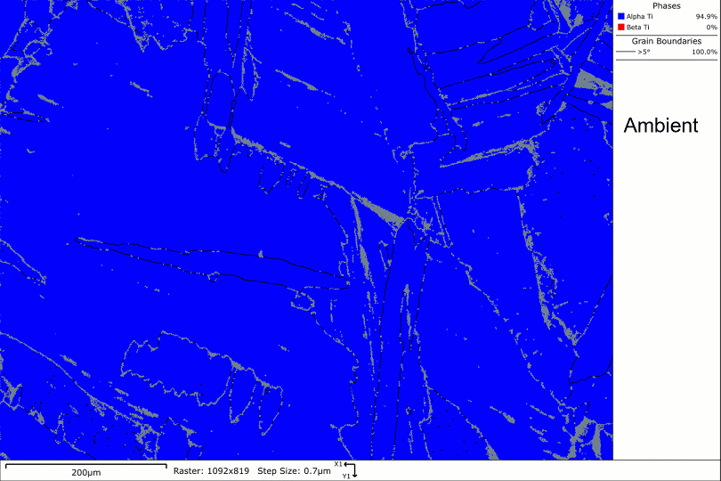
Series of phase maps collected during a high-T EBSD experiment on a Ti sample, showing the phase transformation from α (blue) to β Ti (red). Note that the temperature shown is the heater temperature: the actual sample temperature is estimated to be ~50 °C lower.
Here a commercially pure Ti sample has been heated through the alpha-beta transition, and a series of high resolution EBSD maps have been collected at analysis speeds in excess of 4000 patterns per second. The sequence of phase maps shows the progression of the phase transformation and the relationship to grain boundaries in the alpha phase.
Application notes
Direct Observations of Phase Transformations using High Temperature EBSD
Learn about a new phosphor screen for the Oxford Instruments CMOS EBSD detector range that uses an optical interference filter to block out the infrared signal during high temperature EBSD experiments. This new technology enables faster and more sensitive analyses of microstructural changes measured in-situ at high temperatures.
Download

