EBSD Explained
Techniques
Applications
Hints and Tips
Technology
OXFORD INSTRUMENTS EBSD PRODUCTS
CMOS Detector RangeAZtecHKL Acquisition SoftwareAZtecCrystal Processing Software
Page 1 of 4
Before looking at how the EBSD technique works, it is important to understand the concept of crystallinity and the term “microstructure”.
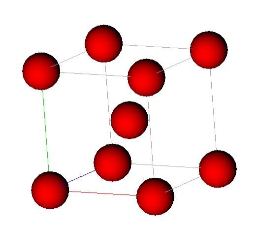
Many familiar materials such as metals, minerals or ceramics are crystalline. In crystalline materials, the atoms that form the material are arranged to repeat periodically in space. The imaginary three-dimensional grid of points on which the atoms sit is called the crystal lattice. Of course, the size of the atoms and the distances between the repeating groups of atoms are tiny. For example, in aluminium, the atoms are arranged at the corners and face centres of a cube. The length of the edge of the cube is 0.405 nanometres - about 200,000 times smaller than the width of a human hair (1 nanometre is 10-9 m).
On the atomic scale, the crystalline structure of material is very regular. Sometimes, the regular crystal lattice is repeated across distances of many millimetres without any change in orientation – these are known as single crystals. An example would be the natural crystals of minerals such as quartz, where the shape and symmetry of the visible crystal reflects the underlying regularity in the atomic structure. Single crystals can also be fabricated: for example, the single crystal silicon wafers used in the semiconductor industry are up to 300 mm wide.

Unit cell for ferrite (BCC Fe) showing atoms at the corners & centre of the cubic unit cell.

Unit cell for cementite (Fe3C) containing iron atoms (red) and carbon atoms (green).

Crystal structure of cementite formed by repeating the unit cell in space.
More often however, the crystal structure is uniform over only short distances and the material is formed of an aggregate of single crystal “grains”. Such material is called “polycrystalline” and the size of the grains can range from nanometres to many centimetres. Even within the individual grains the lattice may not be perfect and can contain defects which have important effects on the behaviour of the material. The crystal lattice orientations vary between the different grains, and so at the interface between the grains we have boundaries which can be defined in terms of the change in orientation from one grain to the next (the “misorientation”).

Material is commonly an aggregate of single crystal grains.

Grain structure visible in a casting.
In many deformed or processed materials, the 3D orientation of the crystal lattices in the different grains is not random. The nature and degree of any alignment of these lattice orientations is known in materials science as “texture” (or in the geological sciences as “crystallographic preferred orientation”). In addition, many materials will contain multiple phases (i.e. materials with different crystal structures), such as the different minerals in a rock or the different structures of iron in a duplex steel.
When we consider the grain assemblage, the phase distribution and the nature of boundaries in a material, along with other microscopic constituents such as pores or inclusions, then we refer to this as the material’s microstructure.
*Image example of a material with a weak texture (before) & a strong texture (after).
Why is the microstructure
important? It is simply because many of the most important physical
characteristics of a material are controlled by the microstructure. We can
think how the strength of a piece of wood will differ markedly when we try and
break it along or across the wood’s grain, and much the same concept applies to
polycrystalline materials. All of the microstructural characteristics will
profoundly affect the bulk material properties, including the strength,
toughness, ductility, corrosion resistance, electrical properties and so on.
So, if we want to understand or control a material’s physical properties, then
we need to be able to characterise the microstructure.