EBSD Explained
Techniques
Applications
Hints and Tips
Technology
OXFORD INSTRUMENTS EBSD PRODUCTS
CMOS Detector RangeAZtecHKL Acquisition SoftwareAZtecCrystal Processing Software
The following model describes the principle features of pattern formation during an Electron Backscatter Diffraction (EBSD) analysis.
A beam of electrons is directed at a point of interest on a tilted
crystalline sample. The electron beam, as it impinges on the sample
surface, is incoherently and quasi-elastically scattered in all
directions from what can be considered a point-like source within the crystal (the size of this incoherent scattering determines the
spatial resolution of the technique and is usually measured in 10s nm).
This scattering forms a divergent source of electrons close to the surface of the sample, and some of these electrons are incident on atomic lattice planes at angles which satisfy the Bragg equation:
nλ = 2dsinθ
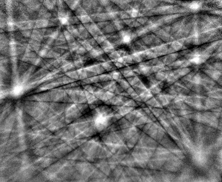
Example EBSP from the trigonal mineral quartz (SiO2), showing the many individual Kikuchi bands that make up the final diffraction pattern.
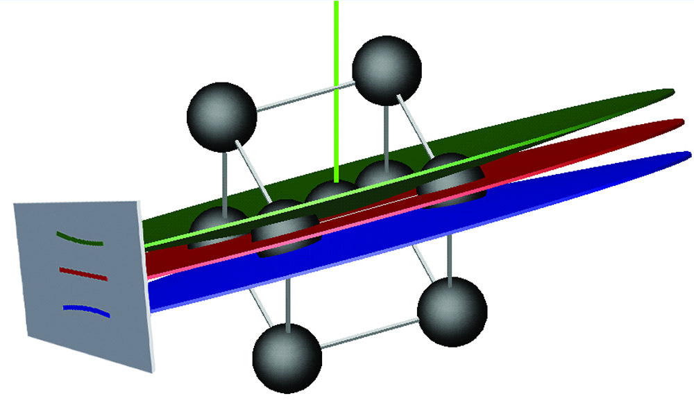
The formation of a Kikuchi band in an electron backscattered diffraction pattern (EBSP).
where n is an integer, λ is the wavelength of the electrons, d is the spacing of the diffracting plane, and θ the angle of incidence of the electrons on the diffracting plane.
These electrons are diffracted to form a set of paired large-angle cones that correspond to each diffracting plane, such as the green and blue cones in the image above, corresponding to a single (110) lattice plane (red disc). The image produced on the EBSD detector (usually using a phosphor screen to convert the electrons to light) contains characteristic Kikuchi bands which are formed where the regions of enhanced electron intensity intersect the screen, as shown both in the schematic image and the example EBSD pattern (left). The pattern imaged by the EBSD detector is a gnomonic projection of the diffracted cone, making the band edges appear hyperbolic.
The mechanisms giving rise to the Kikuchi band intensities and profile shapes are complex. As an approximation, the intensity of a Kikuchi band for the plane (hkl) is given by:

where fi(θ) is the atomic scattering factor for electrons and (xi, yi, zi) are the fractional coordinates in the unit cell for atom i. An experimental diffraction pattern can be compared with a simulated pattern calculated using this equation, in order to ensure that only planes that produce visible Kikuchi bands are used when solving the diffraction pattern. However, in most cases the structure factor approach to calculating band intensities, as outlined above, is sufficient for ranking the intensities of families of lattice planes, and thus for determining the cut-off value for Kikuchi band intensity to be considered during indexing.
Many-beam dynamical simulations are now routinely used to simulate EBSD patterns (for example, for pattern matching or dictionary indexing approaches). This modelling approach is more reliable in determining the intensity variations within a pattern but is computationally much more intensive than a standard kinematical approach, as described above. The example experimental pattern and simulations below highlight the differences between the 2 simulation techniques. However, dynamical simulations are not necessary for determining the Kikuchi band positions and relative intensities (all that is required for standard indexing using the Hough transform), so the kinematical model is still in use for generating the reflector intensities utilised in most routine EBSD analyses.
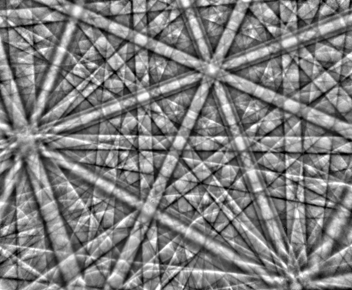
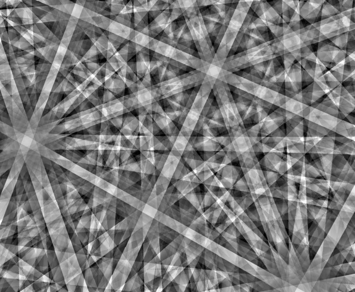
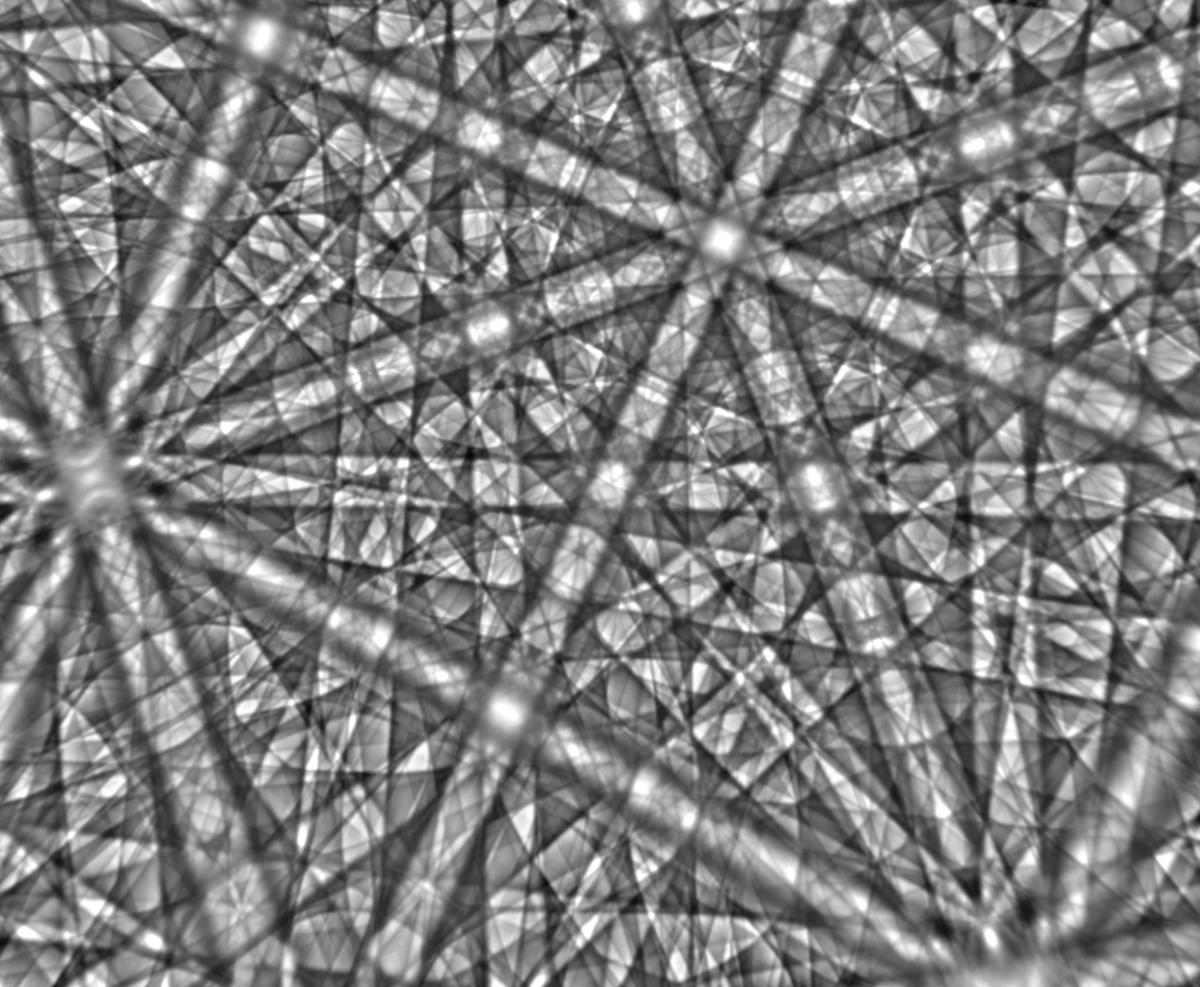
Left - Experimental EBSD pattern from cubic ZrO2. Centre – standard kinematical simulation of the same pattern. Right – many beam dynamical simulation of the same pattern. Simulations courtesy of Aimo Winkelmann.