EBSD Explained
Techniques
Applications
Hints and Tips
Technology
OXFORD INSTRUMENTS EBSD PRODUCTS
CMOS Detector RangeAZtecHKL Acquisition SoftwareAZtecCrystal Processing Software
Once an Electron Backscatter Diffraction (EBSD) system has been calibrated, it is possible to automatically index the diffraction patterns and to calculate the crystal orientation. This is typically accomplished using the following steps:
This whole process is automatic and, for the latest commercial systems installed on modern computers, can take a fraction of a millisecond.
More information about the latest indexing techniques, including methods that use pattern simulations instead of the Hough transform, can be found here.
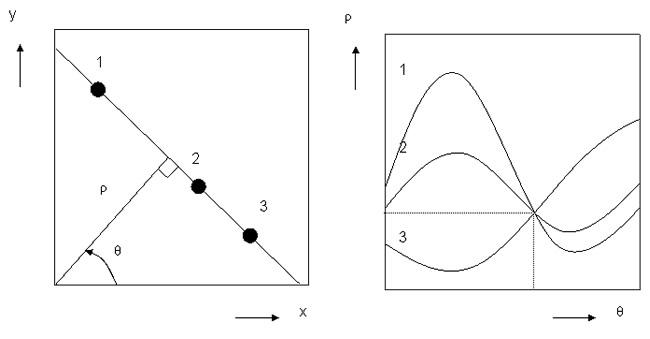
The Hough transform, which identifies the positions of the Kikuchi bands, converts the image from the EBSD camera into a representation in Hough space using the following relationship between the points (x, y) in the diffraction pattern and the coordinates (ρ, θ) of the Hough space:
ρ = x cosθ + y sinθ
A straight line in the image space (x, y) can be characterised by ρ, the perpendicular distance from the line to origin and θ, the angle made with the x-axis, and can be presented by a single point (ρ, θ) in Hough space, as shown in the image.

The Hough transform converts lines into points in Hough space
The Kikuchi bands appear as bright regions or peaks in Hough space, which are easily detected and used to calculate the original band positions. This is shown in the series of images below. It is important to note that the Hough transform is ideally suited to the automated analysis of EBSD patterns (EBSPs), as it is extremely fast and copes well with noisy images.


EBSD pattern indexing using the Hough transform. From left to right: Example EBSP collected from silicon at 20 keV beam energy; The Hough transform image showing the identification of the highest intensity peaks; The corresponding Kikuchi bands in the EBSP (using the same colours); The indexed diffraction pattern (blue cross marks the position of the pattern centre).
This process is fully automated in commercial EBSD systems. The electron beam can therefore be scanned across the surface of the sample in a regular grid of points (typically orthogonal or hexagonal) and, at each point, an EBSP collected and indexed. The phase and orientation information are stored for every point and this allows the microstructure of the sample surface to be reconstructed in the form of phase, orientation, grain or boundary maps (find out about the different ways to display EBSD data here). More information about how these data can be used to characterise sample properties can be found in the Applications section here.