EBSD Explained
Techniques
Applications
Hints and Tips
Technology
OXFORD INSTRUMENTS EBSD PRODUCTS
CMOS Detector RangeAZtecHKL Acquisition SoftwareAZtecCrystal Processing Software
The scanning electron microscope (SEM) electron beam and imaging settings will have a profound effect on the quality of any subsequent Electron Backscatter Diffraction (EBSD) analyses. The resolution of the EBSD technique is primarily influenced by the physics of the diffraction pattern source volume: this is significantly larger (e.g. 10s-100s nm diameter) than the typical spot size of a focused electron beam, especially on a field emission gun SEM. However, the beam energy (i.e. accelerating voltage), beam current and scan settings will all influence the EBSD results.
In addition, some SEMs have a variable pressure (VP) or low vacuum (LV) capability, enabling operation with low levels of gas within the chamber: this can also be very beneficial for EBSD when analysing non conductive materials.
In the tabs below you can read about how to set up and to optimise the SEM conditions in order to get the best EBSD results for a range of applications.
The beam energy, usually set as the accelerating voltage, is probably the most important beam setting since it will control the EBSD pattern (EBSP) source volume. A higher accelerating voltage will increase the pattern source volume (and thus worsen the spatial resolution of the analysis), whereas a lower accelerating voltage will decrease the source volume and improve the resolution. However, lowering the accelerating voltage can have other detrimental effects on the EBSD acquisition:
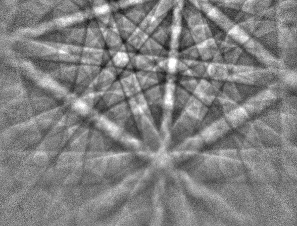
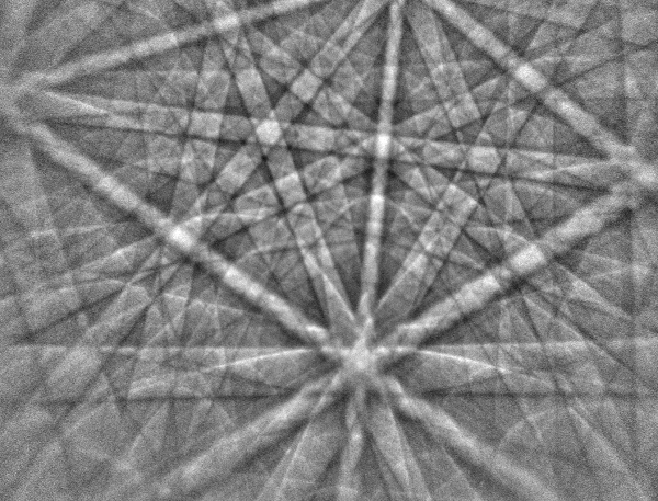
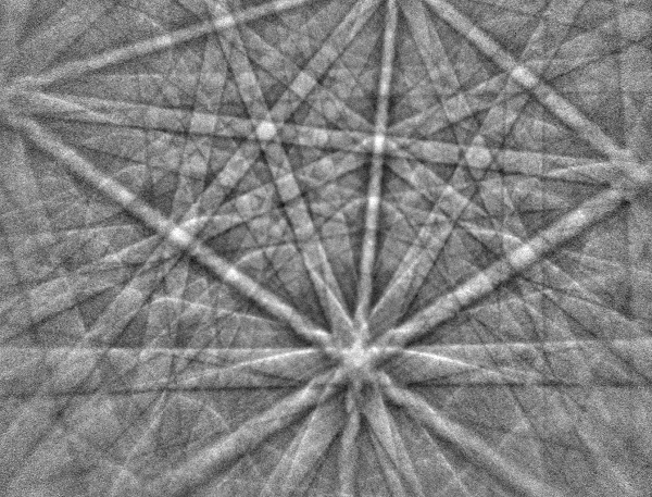
EBSPs collected from a single grain in a steel sample at 10 kV (left), 20 kV (centre) and 30 kV (right). Note that the position of the Kikuchi bands remains constant, but their widths and sharpness change.
For most materials, operating at 20 – 25 kV gives a good compromise between the spatial resolution and a high signal, and enables good quality analyses even if there is a thin oxide layer on the sample surface, or if the sample has a thin conductive coat. However, for nanocrystalline or highly deformed samples it is beneficial to reduce the pattern source volume as much as possible, and results will improve with a reduced beam energy. An example is in the study of martensite: the interstitial carbon distorts the crystal lattice resulting in blurred EBSPs. Reducing the accelerating voltage produces sharper EBSPs and thus better indexing, as shown in the images below.
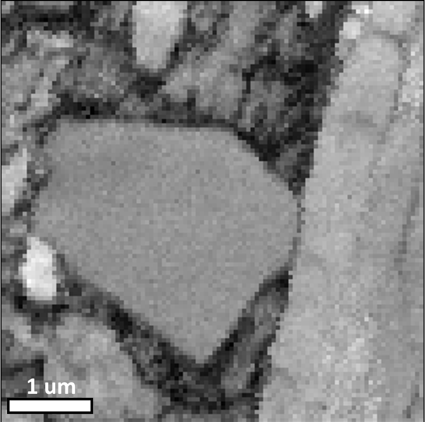
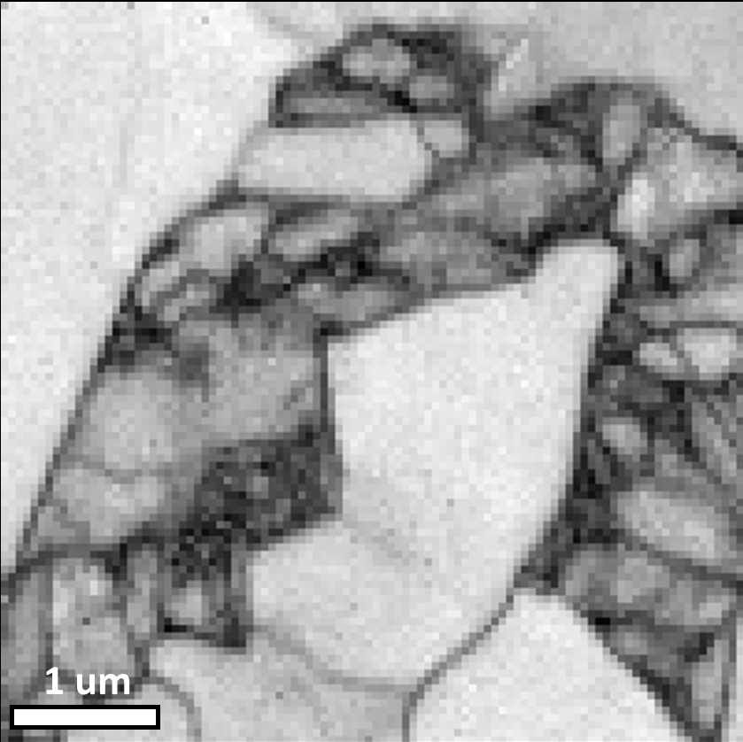
Pattern quality maps from EBSD measurements of a martensitic steel. Left – 20 kV, Right – 10 kV. The lighter shades indicate higher quality patterns in the lower energy analysis, due to the reduced pattern source volume.
Effective EBSD analyses can be achieved down to 5 kV using a conventional EBSD detector: below this, the phosphor efficiency drops markedly and, although analyses are possible, the slow speed makes it impractical. New direct detection technologies coupled with pattern matching indexing approaches may make ultra-low energy EBSD analyses more effective.
For transmission Kikuchi diffraction (TKD), the electron beam needs to pass through the electron transparent sample with minimal beam broadening, and hence a high beam energy is desirable. Although TKD is possible with beam energies of 20 kV or below, it is most effective to use 25-30 kV for the majority of samples.
Beam current is an often mis-represented variable. For most EBSD analyses, the beam current is not a critical value: what is more important is the electron dose (i.e. the beam current x the exposure time at each point). It is the electron dose that will determine if an EBSD pattern has a high enough signal to be indexed to the required level of precision, and in most cases it is the electron dose that will determine if a sample is damaged by the electron beam.
Therefore the beam current (usually measured in nA) will simply determine how fast an analysis can be performed to a given level of data quality. A low beam current (<1 nA) will require longer exposure times and the data acquisition will take longer. This is illustrated by the EBSPs in the image below. Dropping the beam current (from the 1st to the 2nd EBSP) results in a corresponding drop in electron dose, and the signal to noise ratio (SNR) in the pattern will also drop. However, if the exposure time is then increased (3rd EBSP), then the electron dose is the same as in the 1st EBSP, and the SNR is approximately equal.
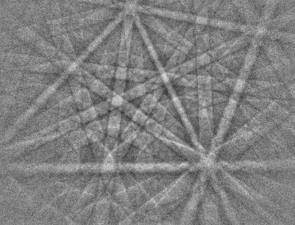
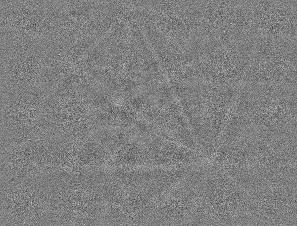
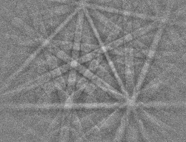
EBSPs collected with different beam conditions and electron doses using an old CCD-based EBSD detector. Left – beam current 2 nA, exposure time 36 ms (total dose 72 nAms). Centre – beam current 200 pA, exposure time 36 ms (total dose 7.2 nAms). Right – beam current 200 pA, exposure time 360 ms (total dose 72 nAms).
There are cases when the beam current is important:
As a general rule of thumb, use a high enough current to maximise the performance of your EBSD detector – for most systems and applications this is in the range of 1-30 nA, but always consider the electron dose.
The highly-tilted geometry that is used for EBSD analyses poses some challenges for imaging the surface of the sample. Unlike when imaging flat samples, for EBSD we need to consider:
In almost all cases it is necessary to apply a tilt correction so that the shapes and areas that are measured in an EBSD map are a true reflection of the real shape / area when imaged in a non tilted geometry. However, if EBSD analyses are being performed on rough samples (such as a fracture surface) or on small rods, whiskers or pillars, then it can be easier to work without tilt correction.
The same applies to dynamic focus. In most cases this will be required in order for the top and bottom of the analysis area (and any resultant EBSD maps) to be in sharp focus; however, if an SEM has a depth of field mode (with a parallel beam) then dynamic focus may not be necessary at higher magnifications.
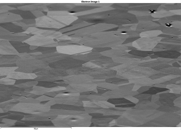

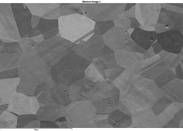
Forescatter images collected from a tilted EBSD sample. Left – no tilt correction or dynamic focus. Centre – tilt corrected but no dynamic focus. Right – both tilt corrected and with dynamic focus.
If working at very low magnifications, then there will be a significant variation in the working distance from the top of the analysis area to the bottom, and there will likely be some additional distortion in the image due to the beam scanning. This can cause problems for EBSD analyses, with peripheral regions not indexing as well and, if multiple fields are being montaged together to form a single dataset, then there will likely be alignment errors at the edges of each field. The severity of the problem will vary from SEM to SEM, but care must be taken when working with very large field of views (i.e. >1 mm across).
Some SEMs have the capacity to introduce additional gas into the chamber (e.g. N2, air or water vapour). Such instruments are usually referred to as variable pressure (VP) or low vacuum (LV) SEMs and are useful because the gas can dissipate the build up of charge on the surface of non-conducting materials.
For EBSD analyses of non-conducting samples, the most common approach is to coat the samples with a thin conductive layer (typically 5-10 nm of carbon). However, EBSD can easily be performed on such samples without requiring any coat, by using a VP/LV instrument.
The optimum pressure will depend on the geometry (the electron path length is critical, so the working distance and detector distance need to be taken into account), the beam energy and the gas type, but in most cases a pressure of 10-30 Pa is sufficient to remove charging effects but maintain good EBSD pattern quality. The example patterns below show how the pattern quality decreases significantly as the chamber pressure increases.
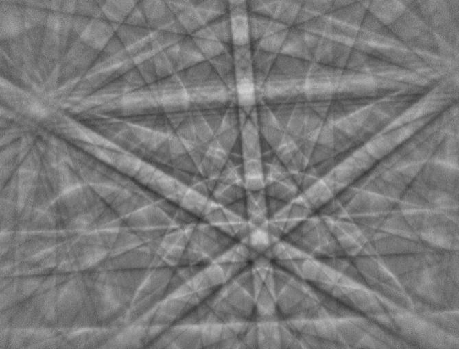
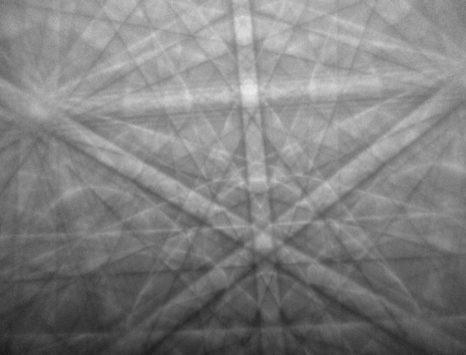
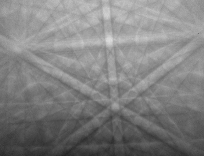
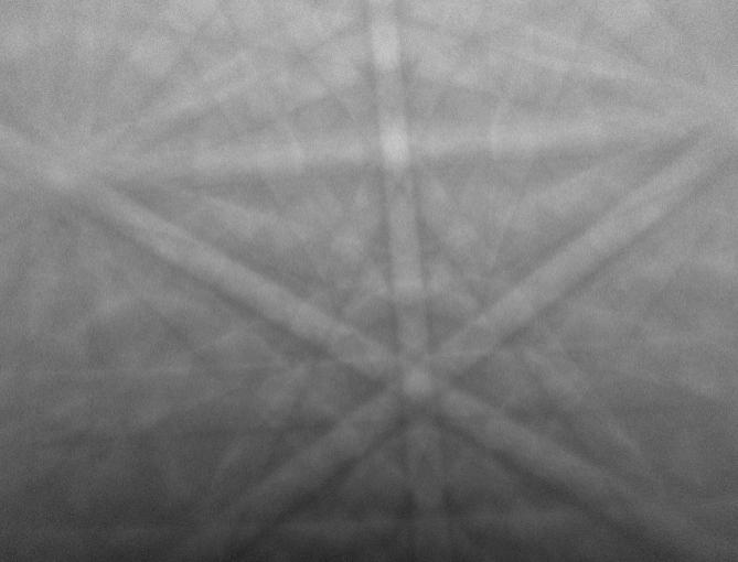
Effect of SEM chamber pressure on EBSP quality from a Ni sample. From Left to Right – High Vacuum (0 Pa); 10 Pa (~0.05 Torr); 70 Pa (~0.5 Torr); 130 Pa (~1 Torr).