EBSD Explained
Techniques
Applications
Hints and Tips
Technology
OXFORD INSTRUMENTS EBSD PRODUCTS
CMOS Detector RangeAZtecHKL Acquisition SoftwareAZtecCrystal Processing Software
Electron Backscatter Diffraction (EBSD) provides information from the sample surface. However, there is often a requirement to get the same type of information from a 3D volume, in order to study grain structures, 3D grain sizes and interface boundaries. Depending on the size of the volume of interest, this can be achieved in several ways: For large scale features it is possible to use mechanical sectioning techniques to expose a new surface at different depths of the sample, and to analyse at these different depths. Alternatively, carefully controlled broad ion beam milling can be used to incrementally remove layers of material. Both of these techniques have recently been automated (in some cases with the use of a robot arm to transfer the sample from the scanning electron microscope (SEM) to the polishing rig), enabling efficient generation of 3D microstructures on the scales of 100s μm to mm.
For smaller scale features, it is not practical to take the sample out of the SEM chamber and then reposition it to collect more data. A solution is to use an SEM combined with a focused ion beam (FIB-SEM), where the ion column is used to mill away the surface between each EBSD map.
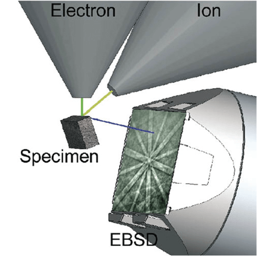
This process is also typically automated. To achieve this the sample must be placed in a geometry suitable for both milling, with the ion beam parallel to the sample surface, and for EBSD data collection.

Geometry set up for automated 3D EBSD using a FIB-SEM. The illustration shows the set-up for the EBSD acquisition step; for the FIB milling, the sample would be rotated 180° and tilted so that the ion beam is parallel to the surface to be analysed.
Depending on the setup it can involve moving the sample automatically between these two working geometries to have an optimum geometry for both (as illustrated in the figure above), whereas on other setups it is done without moving the sample and having a single geometry that allows milling as well as EBSD data acquisition.
By repeating the process of acquiring an EBSD dataset and exposing a new surface, it is possible to generate a 3D representation of the microstructure within the analysed volume. To get good data resolution, it can be necessary to collect data from many tens of slices (potentially more than a hundred).
Although the significant increases in detector technology have dramatically decreased the time taken to acquire 3D EBSD datasets, experiments can still take over 24 hours, given the extensive milling times required. Recent developments in plasma FIB technology and the integration of femtosecond lasers into FIB-SEMs promise further speed advances, with the potential for rapid 3D analyses of volumes significantly exceeding 106 μm3.
One of the major challenges of any 3D EBSD analysis is the reconstruction of data into a full 3D volume, and the extraction of key information from that dataset. Invariably there will be some offset between individual layers, with additional complications arising from sample drift during each EBSD map (although such drift is usually minimised with the use of the latest high-speed CMOS-based EBSD detectors). There may also be variations in the spacings between each slice that need to be compensated for during the reconstruction process.
Once the slices have been aligned and compiled into a full 3D volume, subsequent analyses can extract extremely valuable information that may not be possible using standard 2D measurements. These include 3D grain shapes (as shown in the example below), detailed studies of boundary interfaces and investigations into the distribution of plastic strain (and dislocations) in 3D.
Although there are commercial 3D reconstruction software packages, many researchers utilise the open-source software package Dream 3D.

A 3D EBSD example from a Cu dataset collected with a step size of 0.2 μm in the x, y and z directions, with 51 EBSD slices. Left: Reconstructed and processed 3D orientation map; Centre: Cross-sections in X, Y and Z planes; Right: A single grain selected and highlighted. The full volume is 20 x 18 x 10 μm.